Blog


HIGH-DENSITY INTERCONNECT PCB - PART 1

Published on 17/07/2026

Introduction to HDI Boards (High-Density Interconnect Boards)

HDI (High-Density Interconnect) boards are advanced printed circuit boards (PCBs) designed with fine traces, micro-vias, and high wiring density to meet the demands of modern electronic devices for miniaturization and high performance.

Key Features of HDI Boards

  • High Wiring Density – Trace width/spacing typically less than 100μm (4 mil)
  • Micro-Vias – Via diameter usually smaller than 150μm (6 mil)
  • Multilayer Structure – Manufactured using build-up technology
  • Blind & Buried Vias – Laser drilling enables interlayer connections
  • Thin Design – Dielectric layer thickness can be less than 50μm

HDI Board Manufacturing Processes

  • Laser Drilling – Used to create micro blind and buried vias
  • Via Filling & Plating – Ensures complete conductive material filling
  • Fine-Line Imaging – Advanced exposure and etching techniques
  • Lamination Process – Multiple pressing for multilayer construction
  • Surface Finishing – ENIG (Electroless Nickel Immersion Gold), OSP (Organic Solderability Preservative), etc.
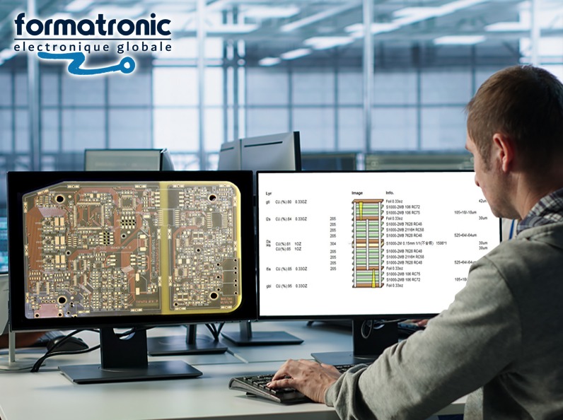
FORMATRONIC, HDI PCB manufacturer


PCB & ENVIRONMENTAL POLICY

Published on 12/05/2026

We strictly comply with all national and local environmental regulations in China, and have established a complete environmental management system covering wastewater treatment, waste gas treatment, solid waste disposal, and hazardous waste management.

  • Wastewater: All production wastewater is treated in our dedicated on-site treatment system to meet discharge standards before being released. 
  • Waste gas: We are equipped with professional waste gas treatment equipment to ensure emissions are within regulatory limits. 
  • Solid & hazardous waste: Hazardous wastes generated from PCB production are classified, stored, and disposed of by qualified and officially licensed professional companies in full accordance with legal requirements.
  • Our factory has obtained relevant environmental certification and regularly accepts government inspections and third-party audits. Environmental protection has always been one of our core management priorities, and we are committed to maintaining clean, compliant, and sustainable production.

    In addition to our standardized wastewater treatment and waste gas treatment systems, our PCB factory has also implemented a full set of environmental protection and sustainable production measures.

    We have established a complete resource recycling system to recycle materials wherever possible during production, greatly reducing resource consumption and waste generation. Meanwhile, we actively promote water conservation and energy-saving initiatives, including water recycling, optimized pipeline design, high-efficiency equipment, and intelligent power management, to minimize water and electricity usage.

    All our environmental protection practices strictly comply with national and local environmental regulations, and we regularly accept official inspections and third-party audits. Environmental protection and sustainable development have long been an important part of our corporate responsibility and production management.

Any question, please contact our team.

PCB & Stencil online store